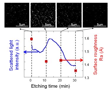
Many studies have reported surface roughness measurements using contact methods such as atomic force microscopy (AFM). However, although this approach can determine surface roughness with sub-nanometer resolution, it is a time-consuming process. Now, a simple non-contact method, based on the detection of scattered light intensity during near-field etching, has been revealed that provides in situ real-time monitoring of changes in surface roughness with angstrom resolution.

A team of scientists from the University of Tokyo, SIGMA KOKI, and the National Institute of Information and Communications Technology (NICT), has developed a non-contact self-organized method of near-field etching that can reduce surface roughness, Ra, to 1.36 Å. This represents a significant advance in the state of the art, as surface roughness below 2 Å has not been demonstrated using conventional chemical-mechanical polishing. More recently, the team performed real-time monitoring of surface roughness during its optical near-field etching process by measuring the intensity of light scattered from the sample.
To their surprise, this method can detect changes in surface roughness with angstrom resolution. Furthermore, it yields in-plane information about the surface as well as the surface roughness. Comparison of the etching-time dependence of the surface roughness and the power spectrum revealed that near-field etching not only decreased the surface roughness, but also increased the number of scatterers, which was confirmed using AFM. Because the intensity of scattered light decreases with decreasing surface roughness, it should be noted that the flattened substrate has a higher laser-damage threshold due to the reduction of scattered loss at the surface.
As this non-contact method does not require a polishing pad, it can be applied not only to flat substrates but also to three-dimensional substrates, which can have convex or concave surfaces, such as micro-lenses and the inner-wall surfaces of cylinders. Further optimization of the etching parameters (wavelength, power density and etching time) should provide scope for an additional reduction in surface roughness. The scientists believe that their latest results, published in the journal Nanotechnology, will accelerate commercialization of this new technique.
About the author
This study was conducted by research teams from the University of Tokyo, SIGMA KOKI Co, Ltd, and the National Institute of Information and Communications Technology, in Tokyo, Japan. The teams are part of a collaborative research unit funded by the New Energy and Industrial Technology Development Organization (NEDO), which is focused on the formation of ultra-flat surfaces using optical near-field techniques. Prof. Takashi Yatsui (University of Tokyo) managed the research and analysed the data obtained by Kazuya Hirata (SIGMA KOKI Co, Ltd), who performed the near-field etching and atomic force microscopy experiments. Prof. Motoichi Ohtsu is head of the Nanophotonics Research Center at the University of Tokyo and guided the project. Yoshinori Tabata (SIGMA KOKI Co, Ltd), Dr Wataru Nomura and Prof. Tadashi Kawazoe (University of Tokyo), and Prof. Makoto Naruse (University of Tokyo and National Institute of Information and Communications Technology) were involved in the discussion of results and contributed to the manuscript.
Sources: http://nanotechweb.org/cws/article/lab/43766